Figure 1A shows the false 2-D plot fs-TA in the mid-IR region with a central detection window of 5000 nm (2000 cm-1) for MAPbBr3 thin film using excitation wavelength of 530 nm. At time zero, an intense positive signal appears due to the population of electrons in the conduction band.24, 28, 39, 42 This transient positive signal decays exponentially towards zero within few nanoseconds. However, the extracted spectra show negative features at longer time scale > 1.0 ns; see Figure 1B. Also, the extracted kinetic trace at 4900 nm shows a multi-exponential decay for the positive signal with an average lifetime of 120 ps, followed by a small negative feature beyond 2 ns; see Figure 1C.
The same film (MAPbBr3) was measured by fs-TA in the visible range, and an extracted kinetic trace at 550 nm corresponding to the ground state bleach (GSA) is compared with the extracted kinetic trace at 4900 nm from the mid-IR region; see Figure 1D and Figure S5. The comparison shows that both normalized kinetic traces from different spectral regions are very similar, except the presence of a new feature at the extracted kinetic trace from the mid-IR range; see Figure 1C-D. The similarity between the two kinetic traces for MAPbBr3 film confirms the validity of mid-IR signal to trace charge dynamics in perovskite films. However, the charge dynamics at in the mid-IR region are not similar. For example, negative features at the red-part of the false 2D plot (4900 nm) in Figure 1A, appears differently than in the blue-part (5120 nm). Extracting a kinetic trace at 5120 nm (1953 cm-1) shows earlier conversion of positive to negative signals at ca. 200 ps; see Figure 1C. Also, comparing this kinetic trace with the one extracted from the GSB in the visible region, shows different behavior than kinetic trace at 4900 nm; see Figure 1D. This highlights the dependence of such negative feature on the probed window.
Upon measuring the iodide-derivative, MAPbI3 film, a detectable fs-TA mid-IR signal was also found, but with different behavior, see Figure 2A-B. Interestingly, the transient mid-IR signal for MAPbI3 film was changing over minutes time scale; see Figure 2C. Thus, various kinetic traces were extracted at different times and compared together at the same proved wavelength. For instance, the fresh-irradiated film (0 min.), appositive signal was measured until ca. 100 ps, and then a small negative signal started to emerge. The disappearance of the positive signal became faster with the longer the exposure process associated with an increase of the signal at early times; see Figure 2C. For example, at 26 minute of irradiation, the positive signal converted into a negative signal within 10 ps; see Figure 2C. Interestingly, this process is reversible, in which switching off the irradiation for almost 8 minutes, and re-measure the dynamics again at the same irradiated spot (@34 minutes in the Figure 2C), the dynamics slowly started to be similar to the 10 minutes measurements; see Figure 2C. Moreover, after the appearance of the negative signal it decays later on to zero due to the recombination process, see Figure 2C.
Upon measuring the same film in the visible range, a strong GSB signal at ca. 760 nm was observed overlapping with an ESA spectra extending from 650 to 850 nm, see Figure S7. However, no unique change in dynamics has been observed in the visible range similar to the shown data in the mid-IR range. And upon comparing the extracted normalized visible kinetic trace at 760 nm with the ones from the mid-IR, it is evident the visible kinetic trace is similar to the one from mid-IR at 26 min only at early times; see Figure 2D. However, still at later times, the mid-IR signal switches its sign, but not the visible kinetic trace at 760 nm. The change of charge dynamics upon irradiation has been assigned in iodide-rich perovskite materials to halide-defects assisted by the low energy needed for defects formation.14, 43-45
This comparison highlights that this appearance of negative features in the mid-IR region is a dynamical process and also reversible (MAPbI3 case). Additionally, the extracted kinetic trace at 4900 nm from the MAPbI3 shows stronger and earlier negative signal than the one shown in MAPbBr3 case. Moreover, for further confirmation of the working conditions, a reference silicon wafer substrate was measured under the same procedure, and no negative features have been detected, see Figure S8. Thus, we assign these strong negative signatures in the mid-IR for MAPbI3 film to the emissive trapping process near the VB of perovskites, in which the mid-IR signal is more sensitive than in the visible range. Several studies showed that iodide based perovskites are more vulnerable for formation of more trap states than bromide ones.1, 8, 14, 23
To scrutinize our interpretation about the sensitivity of mid-IR towards trapping process, we performed the same measurements on other perovskite films including FAPbBr3, FAPbI3 and mixture of their halides. For the FAPbBr3 film, the mid-IR signal shows primarily a strong negative signal close to time zero converting into a positive signal with a lifetime of ca. 60 fs, which has been assigned to the exciton thermalization/dissociation process7; see Figure 3A-B. Previously, in the MAPbBr3 film, exciton binding energy seems to be smaller, thus, no detection of exciton dissociation process could be seen; see Figure 1. Then the charge recombination in the FAPbBr3 film (decay of the TA signal) has been fitted with multi exponential behavior, giving an average lifetime is about 10 ps, see Figure 3B.
For the FAPbI3 film, similar observation was estimated for the lifetime needed for exciton dissociation in FAPbI3 film; see Figure 3C-D. However, instead of charge recombination, the signal converted again to a negative signal due to a trapping process of time component ca. 8.5 ps; see Figure 3D. Then the trapped electrons recombine slowly with a lifetime higher than 1 ns. It is clear that this negative signature in the mid-IR range is associated with the iodide derivative of hybrid perovskite films due to the presence of trapping centers in the iodide perovskites more than in bromide perovskites.
To verify the role of iodide anion for the formation of emissive trapping centers, we synthesized other set of various perovskite films of different ratios between the iodide and bromide halides (MAPbInBr3-n) to investigate the effect of doping with iodide ions on the presence of such negative signal. Figure 4A shows the kinetic traces of mid-IR signals for four films of MAPbInBr3-n, in which n varies from 0 to 3. The extracted kinetics at 4900 nm show the appearance of negative signals at different times ranging from 100 ps to 1 ns depending on the amount of iodide halide present, in which higher content of iodide shows faster appearance of negative mid-IR signal. Thus, the iodide content in perovskite films controls the appearance of the negative signal (emission of mid-IR).
To study the dependence of appearance of these negative signals on the energy of the mid-IR probe, the MAPbI3 film is excited at 520 nm (300 µW), and probed at various mid-IR energy ranging from 4000 nm to 6000 nm, as shown in Figure 4B. As expected, the appearance time of the negative signal depends on the utilized mid-IR energy, in which the switching points from positive to negative signal happen at ca. 500 ps when using 4000 nm and at ca. 20 ps upon using 6000 nm. This also illustrates the incapability of visible probe light to directly track the trapping process due the high energy carried by the photons used.
Furthermore, by changing the excitation wavelength from 410 nm to 520 nm for another MAPbI3 film, the extracted kinetic traces at 4500 nm show a dependence of the kinetic decay with the wavelength used; see Figure 4C. The appearance of negative signal is faster upon using 410 nm then became slower with 440 nm, and 520 nm respectively. Upon using the excitation light at 520 nm, the kinetic trace decay to zero with no signature of negative signal, despite that higher power was used, almost 20 times higher (300 µW) than in 410 nm; see Figure 4C. This excitation energy dependence shows that the higher the electron can be promoted in the excited state, the higher than chances to be trapped.
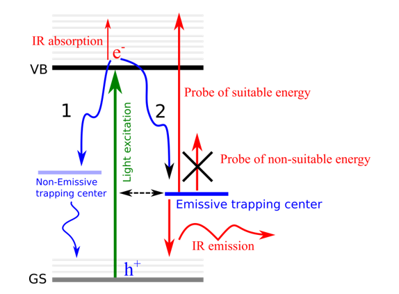
From the above mid-IR transient measurements, the following mechanism can be drawn, see Scheme 1. Upon exciting the perovskite film, the electron in the CB should absorb the following mid-IR probe to populate various vibrational levels in the excited state, giving a positive transient absorption signal. Due to the presence of trap states within the bandgap of the perovskite film, the electron in the CB decays non-radiatively to the ground state, in which the transient signal decays to zero. Interestingly, upon using synthesizing perovskite films using chemical species such as MA+ or I- or both of them as in MAPbI3, negative transient signal in the mid-IR region starts to appear. And since perovskite films have no characteristic features in this mid-IR region, this negative transient signal can be only due to emission of mid-IR signal. It is already established in the literature that MA/iodide perovskite films show more potential to form trap states than other derivatives (FA/Br).1, 23 Thus, we postulate that in MAPbI3 films, different kind of emissive trap states are additionally formed related to ion migration and new phonon modes in these films that are not present for instance in the FAPbBr3 films.1, 23, 46
Interestingly, to detect these mid-IR emissive states suitable probe energy should utilized as shown in Figure 4B. These data presents the influence of the energy carried by the probing photons to free the trapped electrons if sufficient energy is present. For instance, the probed pulse at 4000 nm (2500 cm-1) can liberate the trapped electron more efficient than at 6000 nm (1666 cm-1), and the appearance of negative signal upon using 4000 nm (2500 cm-1) will not appear unless the electron is deeply trapped. In the same way, the appearance of negative signal at 6000 nm (1666 cm-1) is much faster due to lower energy carried by the probe pulse to liberate the trapped electron in the emissive states, allowing for deactivation through the other non-emissive states. These observations are consistent with a previously proposed mechanism that trapped electrons can be excited thermally if the energy difference between the trap state and the CB is small, < 50 meV.20 This also illustrates the incapability of transient absorption in the visible region to detect such a trapping process due to the higher energy carried by the visible probed light, that have the potential to liberate the trapped carriers into higher excited state, producing undistinguishable signal for the trapping process in the visible region.
Moreover, upon using higher band-gap excitations such as 410 nm, the probability of electron trapping in these emissive states is increased despite the excitation intensity used, matching with the expected distribution for the states of trap-density present. We also show that continuous irradiation at high excitation energy for the MAPbI3 film (Figure 2C) increases the rate of trapping (channel 2 in Scheme 1), as well as the intensity of the transient signal. This indicates towards the exciting correlation between the light irradiation and ion migration process in perovskite films.47 This means that changes in the perovskite lattice by the incident light (depending on energy) can lead to the formation of these emissive states.