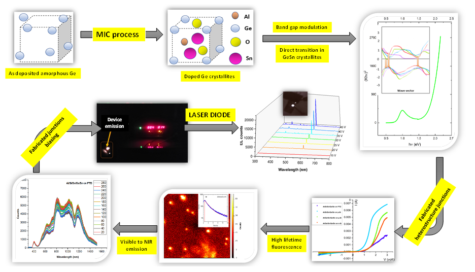
Solubility of Sn in Ge has the most impact in the emission characteristics of direct band gap GeSn alloy. Here, we employed the metal induced crystallization (MIC) process of amorphous Ge and Si via Sn as a novel mechanism to incorporate Sn inside Ge and Si networks. (Al/Si/Sn/Ge/Sn) and (Al/Ge/Sn/Ge/Sn) multilayers are deposited by thermal vacuum evaporation on different substrates. The devices are annealed under low vacuum at 500 ºC. The Ge doped nanocrystals structure is investigated. The direct transition and band gap values have been estimated using diffuse reflectance spectroscopy and Photoluminescence (PL) measurements. PL indicted that the junctions have emissions from visible to NIR regions that make them promise in white light laser sources as well as waveguiding applications. Charge carrier lifetime and EL measurements show high lifetime and very sharp emission, respectively indicating that the prepared structure is a candidate for white laser diode applications.
Research Article
Towards white light laser emission based on strained Poly:(Si/Ge)
https://doi.org/10.21203/rs.3.rs-1406504/v1
This work is licensed under a CC BY 4.0 License
Version 1
posted
You are reading this latest preprint version
Integrated light sources and optoelectronic waveguides open the field to transfer electrical signal via light instead of copper wires to open the era of terahertz data transfer [1]. Researchers encounter challenges in the epitaxial growth of GeSn due to the lattice mismatching between Ge and Sn due to the low solubility of Sn in Ge. Solubility of Sn in Ge judge the emission of GeSn alloys [2]. More incorporation of Sn causes tensile strain in the germanium and transforms the indirect band to a direct one [3]. Abo Ghazala et al. employed Sn for inducing crystallization of the amorphous silicon layer forming nanocrystalline silicon with a direct transition bandgap [4]. Oehme et al. fabricated Ge based LED devices via epitaxial growth on silicon substrates with emission peak in NIR at 1590 nm due to the direct transition of GeSn [5]. Gallagher et al. studied the impact of Sn content on the phase mismatching, dislocation and transformation from indirect to direct transition. They found that with increasing Sn content, dislocations decrease and thus the carrier recombination lifetime increases. This reduced the non-radiative charge carrier recombination [6]. Yiyin Zhou et al. investigated that the emission of GeSn decreases with increasing the temperature over the range from 77 K to 300 K [7]. Ghetmiri et al. studied the effect of temperature and Sn content on PL measurements simultaneously. They found that 4% of Sn content leads to direct and indirect transitions and when the temperature increases up to 300 K, the indirect transition peak began to disappear [8]. Also, there were some trails [9] on increasing the tensile stain in Ge network for the direct transition via the geometry of the epitaxial layers. Since the planar epitaxial growth of GeSn on Ge increases the compressive strain in Ge network due to the mismatching between Ge and GeSn that transforms the transition to indirect again. Huang et al. employed ion etched Si base substrate as a curved layer caused uniaxial strain on Ge layer network [9]. Rainko et al. prepared GeSn micro discs on cone shaped Ge layer using electron beam photolithography [10]. Wirths et al. deposited GeSn layer with 12.5% Sn content on Ge/Si layers. PL measurements revealed that the structure has intense narrow band emission made the structure can be used as a lasing medium [11].
In this work, we employed Sn induced crystallization of amorphous germanium as a mechanism of Sn incorporation to increase the tensile strain in Ge networks fabricated by thermal evaporation technique instead of CVD and epitaxial complicated reactors. The effect of different base substrates as a novel mechanism on the Sn incorporation is investigated. The carrier recombination lifetime with emission at visible and NIR spectral regions is also recorded and interpreted.
- Structural analysis of the prepared configurations on different substrates:
Many attempts were employed in transform the deposited amorphous germanium to poly:Ge via metal induced crystallization process using some metals such as aluminum [12]. Metal induced crystallization occurs when a layer of metal (low melting point) such as Al covered by a semiconductor (SC) layer (high melting point) such as Si and Ge. When the two layers annealed at a temperature that is lower than the crystallization temperature of the semiconductor, the metal layer begins to melt, which causes the semiconducting layer starting to dissolve and diffuse into the metal layer [13] and the dissolved (SC) atoms nucleate. These nuclei conglomerate on each other forming islands of poly:(SC) as shown in the schematic diagram in Fig. 6. Here, we used two different configurations of multilayers on different substrates. Al and Sn are involved to initiate the MIC process and be incorporated in Si and Ge networks.
Figure 1a shows the FESEM micrographs of (Al/Si/Sn/Ge/Sn) and (Al/Ge/Sn/Ge/Sn) multilayers configurations on different substrates. It is observed that the nucleation starts laterally in the sample on the FTO substrate but in the other structure on p-Si, these nuclei start to conglomerate vertically forming hills like shapes of both poly:Si and poly:Ge doped with Sn [14]. The conglomeration increases in the sample deposited on p-Si due to the highly doped base substrate that estimate the aluminum to rapidly diffuse in the Si layer and accelerates the rate of MIC process [43]. It is seen that the rate of crystallization in Al/Ge/Sn/Ge/Sn configuration is increased than the other configurations that involves both Si and Ge. This is because Si has a higher crystallization temperature than Ge, so the rate of crystallization in Ge is higher [15]. The films began to form a continuous Poly:Ge crystallites doped with Sn. It is also observed that the configuration that is deposited on p-Si has smaller grain boundaries than the other on FTO due to the effect of p-Si highly doped substrate that accelerates the diffusion of Al atoms and increases the crystallization of Ge doped Sn as discussed above. These smaller grain boundaries areas increase the charge carrier mobility and the structure becomes suitable for optoelectronic applications [16].
Energy dispersion X-ray analysis asserts the existence of Al, Si, Ge and Sn elements that forms the junctions. It showed also the appearance of Oxygen atoms as a result of the annealing temperature with low vacuum conditions of the value 4×10− 2 mbar. This caused a growth of GeO2 crystallites that give the sample good emission properties along the visible region of spectra as we will discuss later in XRD and Photoluminescence analyses. XRD analysis is carried out to investigate the growth of germanium and silicon nanocrystals and GeSn crystallites as shown in Fig. 1b which shows the existence of GeSn peaks with different orientations in different planes: (111) at 2θ = 27.5° [17], (220) at 2θ = 62.5° [18] and (004) at 2θ = 64° [18]. Ge (220) peak is observed at 2θ = 46° (JCPDS card No. 65–0333) in the sample of the second configuration and disappeared in the first configuration as the second configuration is rich with germanium [17]. Ge (311) (JCPDS card No. 65–0333) is detected at 2θ = 56° for both configurations [17]. Si (111) appears at 2θ = 28.5° (JCPDS card no. 01-079-0613) in the first configuration due to the occurrence of MIC forming poly: Si [4]. There are other three peaks at 2θ = 34°, 38° and 44° corresponding to SnO2 (101), SnO2 (200) (JCPDS Card No 41-1445) and GeO2 (201) JCPDS (card no. 43-1016), respectively due to the annealing at slightly low level of vacuum that causes partially oxidation of Ge and Sn [19, 20]. On the other hand, the configurations deposited on n- Si and p-Si show highly oriented poly-GeSn crystallites at (400) direction of 2θ = 62°. This is due to the effect of single crystalline silicon base substrates as a seed layer that has one direction of crystal growth [21]. It is observed that the intensity of the GeSn peak in the samples deposited on p-Si is higher than the other one deposited on n-Si. This behavior can be attributed to the diffusion of Al atoms away from highly doped p-Si substrate and diffuse in Ge and Si layers which leads to an increase of the rate of MIC. There is a very weak peak of GeSn (004) for the samples on p-Si at 2θ = 64°. XRD analyses show the growth of Ge with a lattice constant = 5.506 Å and 5.57 Å at different orientations for Al/Si/Sn/Ge/Sn and Al/Ge/Sn/Ge/Sn prepared on FTO respectively. In both configurations that prepared on FTO, it is observed that there is incorporation of Sn inside Ge network that causes the growth of GeSn crystallites with different orientations for both configurations [6, 17]. As a result of interstitial incorporation, the lattice constants of the different orientation growth of Ge increased to positive tensile strained for GeSn up to 5.96 Å for the growth direction of plane (400) since the lattice constant of Sn = 6.49 Å is higher than the germanium [22]. It causes a tensile force inside Ge network which increased the lattice constant as mentioned [17]. On the other hand, it is observed the preferred high orientation of the growth of the strained GeSn is associated with an increase of the lattice constant up to 6.06 Å (See supplementary Table S1), which refer to higher incorporation of Sn inside Ge network. This mostly leads to a one direction crystal growth, which increases the electron mobility than the growth in many orientations [23]. The higher strain in the Ge network modulates the valley of the valence band to be aligned with the bottom of conduction band yields modulation of the indirect band gap to direct one [5, 8]. Figure 1c shows the Raman spectra of the fabricated heterostructures. It is observed that for the Al/Si/Sn/Ge/Sn on p-Si device, there is a peak at 500–510 cm− 1 due to the existence of aluminum and tin induced crystallization of amorphous silicon to form poly:Si [24]. The peak at 520 cm− 1 is due to the crystalline p-Si wafer [24]. SiGe is observed at around 390–400 cm− 1 as a result of the alloying between Si and Ge at the high annealing temperature [24]. An appearance of Poly:Ge and GeSn modes are detected at 300 cm− 1 and 270 cm− 1 respectively, which may be due to the transform of the amorphous germanium layer to polycrystalline one via tin induced crystallization and incorporation of Sn metal inside Ge network [25]. The figure also shows two peaks at 180 cm− 1 and 120 cm− 1 that are due to Sn-Sn and SnO respectively [26]. For the heterostructures of Al/Ge/Sn/Ge/Sn on p-Si and n-Si, a peak of NC: Si appeared at 520 cm− 1, which is due to the n type or p type silicon substrates. There are other modes appear at 300 cm− 1 and 270 cm− 1 that are corresponding to poly:Ge and GeSn. Other modes at 180 cm− 1 and 120 cm− 1 refer to Sn and SnO as observed in XRD analysis. Raman confocal microscope images of the fabricated heterostructures are used to investigate the effect of different substrates on the crystallization rate. For the heterostructure of Al/Si/Sn/Ge/Sn on p-Si, the formation of islands of the doped crystallites for both Si and Ge with different colors is observed which may be due to the metal induced crystallization of the deposited amorphous Si and Ge via aluminum and tin. For Al/Ge/Sn/Ge/Sn, the formed clusters are due to Ge nanocrystals as discussed in FESEM images (See supplementary figure S2).
- Direct transition investigation using diffuse reflectance spectroscopy, PL measurements at different cooling temperatures.
As a result of the long-time annealing (24 h) at 500 ºC, Al and Sn are interstitially existing in the Si and Ge networks. These metals incorporation inside Ge and Si modulate the optical energy gaps of these IV group indirect transition semiconductors and the direct optical transition occurs [3, 4]. Figure 2(a) I, II, III, IV and V shows the plot of (Khʋ)2 versus hʋ using modified Kubelka-Munk model of the heterostructures of micro-strained poly-germanium doped with Al and Sn on n-Si, p-Si and FTO, respectively. The higher observed absorption for the heterostructures that interfaces p-Si and FTO substrates than the other one on n-Si. This can be explained as mentioned before: In the heterostructure on FTO, the diffusion rate of metals in Ge is higher since the surface area of interaction between Ge and metal layers increases as a result of the change in morphology of the FTO bottom layer as a result of the high annealing temperature near its melting point. In the case of heterostructure on p-Si, the Al atoms doesn't segregate in the p-doped substrate but these atoms of Al layer are rapidly segregating in the lower majority carriers concentration intrinsic Ge layer and thus increase the rate of crystallization and incorporation of Sn increasing GeSn direct allowed transition [27]. A direct transition of GeO for all heterostructures is ranged between 1.15 to 1.85 eV due to different level of oxygen incorporation in the samples [27]. Another direct transition at Ge crystallites of higher level of oxidation is around 2.02 up to 2.73 eV occurs in the structures prepared on FTO and p-Si substrates. This was suggested due to the diffusion of oxygen atoms of FTO layer in Ge layers under the influence of the annealing that causes vacancies in FTO layer and the low level of vacuum during annealing of the rapid diffusion of multilayers that is on p-Si substrate [28, 29]. Direct transition in the strained GeSn crystallites in all samples is ranged between 0.43 up to 0.61 eV (See supplementary Table S2). These direct transitions at different regions of the visible and near infrared spectrum give these heterostructures good chance in optoelectronic devices applications. The bulk germanium has emission spectra at around 1400–1600 nm. The bulk GeSn alloy has emission at NIR 1800–2200 nm [30, 10]. These ranges of emission may be shifted towards the blue region as the effect of oxidation level [31]. Photoluminescence emission measurements of the prepared heterostructures based on the tensile strained Ge nanocrystals show emission peaks at different regions from the violet light to NIR (Fig. 2b). Two GeOx peaks, the violet peak at 402 nm is due to the oxidation of Ge which is resulted from the annealing at low vacuum up to 10− 2 mbar. The oxidation of Ge shifts the germanium emission to the short wavelengths [32]. Another green peak of GeOx is 514 nm. A red peak at 790 nm is due to lower degree of oxidation as shown in Figure (2b I) [33]. Figures (2b II) shows a broad peak at around 1223 nm in NIR region. It is due to Ge doped with Sn forming GeSn strained nanocrystals [34]. It is observed that the 790 nm and 1223 nm peaks disappear; the 402 nm violet peak and the 514 nm green peak are shifted towards the red region for the prepared Al/Ge/Sn/Ge/Sn on n-Si heterostructure. It is due to the lower rate of MIC process than other samples prepared on p-Si and FTO substrates and hence lower incorporation of oxygen and tin in Ge lattice as mentioned in structural measurements. It is observed a higher emission intensity for both Al/Si/Sn/Ge/Sn and Al/Si/Sn/Ge/Sn heterostructures on p-Si and FTO that increases the rate of MIC process and forming NC:Ge and strained GeSn structures. Figure 2c shows the emission of the prepared configurations on different substrates at different cooling temperatures from 280 K to 20 K. The intensity of the peaks increased with the decreasing of the temperature down to 20 K. This confirms the direct transition occurrence and increasing the radiative recombination [35]. When the temperature is decreased, it enhances the radiative nonthermally transitions [36]. The Al/Si/Sn/Ge/Sn on FTO or p-Si show lower intensity than the Al/Ge/Sn/Ge/Sn on FTO since the second one is rich with germanium. The peak at around 1200 nm in NIR region has higher intensity in Al/Si/Sn/Ge/Sn on FTO and p-Si than the Al/Ge/Sn/Ge/Sn on FTO as a result of the higher solubility of Sn in Ge than its solubility in Si [37]. This will increase the incorporation of Sn in Ge lattice away from silicon causing high intense GeSn peak [38]. The heterostructure of Al/Si/Sn/Ge/Sn on FTO has a continuous wide emission spectra from the visible to NIR region than other structure of the same configuration on p-Si that has its emission mostly in NIR region as a result of the various oxidation levels due to the diffusion of oxygen atoms from FTO layer into the above layers as discussed throughout this article.
- I-V characteristics of the fabricated heterostructures junctions under dark conditions
The diode parameters such as ideality factor n, saturation current Is, threshold voltage Vth and the barrier height are calculated using Schottky Eq. (1) [39] and Richardson Eq. (2) [40].
ID = Is[\({e}^{\frac{VD}{nKT}}-1]\) (1)
 (2)
(2)
The measured IV characteristics are carried out at room temperature in the range of -3 volt to + 3 volts. We obtained four diode junctions of the prepared heterostructures of the two prepared configurations on p-Si, n-Si and FTO substrates as shown in Fig. 3a. Table S3 summarizes the calculated parameters of the prepared junctions. The figure shows that there is no avalanche effect in the reverse biasing of the prepared junctions and a very small dark current in the order of 10− 4 A. This makes the junctions able to use in rectification applications [5, 41]. The ideality factor n is calculated using Schottky equation from the plot of Ln I versus V as shown in Fig. 3b. The values of the ideality factor of the junctions in low voltage biasing region (Region 1) are around 1 near the value for ideal diode structure. However, in the high voltage biasing region up to ± 3 volt (Region 2), the values of the ideality factors are in range of 6 to 35 that are far from the ideal value. This may be due to the tunneling of conduction electrons inside the cloud of metals that contains vacancies in which electrons recombine [5, 42]. From the values of the ideality factor, we can observe the effect of the substrate as mentioned in Raman analyses. In both configurations on p-Si substrate, Al atoms are segregated away from the highly doped p-Si wafer inside Si or Ge networks that cause the trapping effect at the low or high voltage biasing regions. Since the samples have very low dark leakage current that contributes as a noise current [43], they have good opportunity in photodetection applications. Rectification ratio RR calculations refers that the Al/Ge/Sn/Ge/Sn on (n-Si) substrate has lower dark current and higher rectification ratio near 100 that make this heterostructure is a promising junction in photodetection application. The barrier height values indicate that the samples can be detected in near infrared NIR region since the height of the barrier is in the range of 0.6 to 0.8 eV for all samples [44].
- Fluorescence charge carrier lifetime investigation:
Figure 4a shows the raw FLIM data for Al/Si/Sn/Ge/Sn and Al/Ge/Sn/Ge/Sn on FTO, p-Si and n-Si substrates. Photoluminescence intensity shows a decay curve for all the heterostructures. The FLIM images of the samples agree with the densities of the prepared samples that is investigated in PL spectroscopy measurements. Both PL spectroscopy and FLIM images show the highest intensity of emission is corresponding to Al/Si/Sn/Ge/Sn on p-Si heterostructure and the lowest emission is corresponding to Al/Ge/Sn/Ge/Sn on n-Si heterostructure. Figure 4b shows the phasor plot for the prepared heterostructures. It gives a representation of the intensity decays for the corresponding FLIM image shown in the left panel of the figure. In the phasor plot, each pixel in the FLIM image is represented in a 2D diagram with two coordinates namely, S and G. The two coordinates based on the phase shift (φ) between the transmitted wave and the resulting PL wave and demodulation factor (m) in the lase source. The S and G components are given by the following equation [45, 46]:
 (3)
(3)
where τ is the lifetime and ω=2πf is the laser modulation angular frequency (80 MHz). From Eq.4, the lifetime
 (4)
(4)
The phasor plot for the prepared heterostructures showed a cluster of point located at the edge of the phasor plot semicircle, indicating that the prepared samples decay is single exponential decay with an average lifetime ranged between 2.22 up to 2.73 ns as calculated from Eq. 4 (See Fig. 4b)). This charge carrier lifetime of GeSn prepared structures is suitable for diode lasing application compared to B. Julsgaard 2020 [47] and S. De Cesari 2019 [48].
- EL measurements of the prepared white LED of the two configurations.
As EL measurements show that the heterostructures emit different wavelengths along the visible spectra region when we applied 11.6 V on one of these junctions and emitted white light. EL measurements show the emission of the prepared Al/Si/Sn/Ge/Sn configuration at visible and NIR (See Fig. 5a). This configuration has higher emission at NIR region due to the more Sn incorporation in GeSn as discussed before. The second configuration Al/Ge/Sn/Ge/Sn has intense EL emission than the other configuration as it is rich with germanium layers. The prepared configurations can be used as a white light emitting diode at low voltage as shown in Fig. 5b. When we increased the voltage from 15 V up to 45 V, the emission increases and very sharp peaks appear along the spectrum from 300 nm to 800 nm (See Fig. 5c and d). The main peak is at about 590 nm with very high intensity that is the main transition discussed in UV-Vis spectroscopy analysis. It gives these samples the chance to act as a white light laser diode media [49] with very small line broadening. The FWHM is equal 2.168 nm or 1.74 meV.
- Multilayers deposition:
Multilayers of Al/Si/Sn/Ge/Sn and Al/Ge/Sn/Ge/Sn are deposited by thermal vacuum evaporator EDWARDS E306A with thicknesses 100/250/100/250/100 nm and 100/250/100/250/100 nm respectively under a diffusion pump high vacuum of 6×10− 5 mbar on n-Si, p-Si and FTO substrates using triple tungsten spiral to bear such a high current that can give sufficient energy to dissociate any semiconducting elements even the high melting silicon metal as shown in Fig. 6.
- Heterostructures device formation:
These multilayers with different configurations on the above-mentioned substrates are annealed under vacuum conditions of the value 4×10− 2 mbar using vacuumed cylindrical chamber by Edwards rotary pump. The devices are annealed by a controlled heater installed inside the vacuumed chamber and set at 500°C for 24 h as an optimum annealing time after many trials to get well Sn incorporated large grains of poly-Ge and poly-Si. The incorporation of metals such as Sn and Al and formation of micro-strained Si and Ge networks accelerated the MIC process [4] at lower temperature not by the traditional alloying method that requires preparation of GeSn or SiSn as the first step then depositing by epitaxial growth complicated reactors. These heterostructures forming p-n junctions was then coated by grid back and front contacts of Silver metals for the electrical measurements.
- Structural and optoelectronic characterizations:
Structural characterizations and crystal growth of micro-strained Ge and Si are investigated using (D2 BRUKER X-rays diffractometer), Witec Raman confocal microscope with excitation laser wavelength of 352 nm and FE-SEM QUANTA FEG250. Direct band gap investigation and band gap values are calculated using UV-Vis-NIR Diffuse reflectance spectrophotometer JASCO V-770. I-V characteristics of the fabricated junctions and diode parameters calculations are carried out using Potentiostat METROHM Autolab 87070. Spectral emission of the prepared heterostructures. Photoluminescence spectrometers (KIMNON KOHA CO., LTD., JAPAN) with striking He-Cd continuous wave laser beam of wavelength 325 nm and Electroluminescence measurements are carried out using a biasing power supply and a CCD spectra detection camera in the range between 300 nm and 1500 nm.
- Fluorescence charge carrier lifetime setup:
Fluorescence lifetime images are acquired using FLIM system (ALBA v5 from ISS). The excitation is from a laser diode with wavelength of 445 nm coupled with scanning module (ISS) through multiband dichroic filter to Epifluorescence microscope (Olympus, Model IX73) with UPLSA 60X objective 1.2 NA, 0.28 mm wd. Emission is observed and detected by cooled low noise (below 100 counts/sec) time correlated single photon counting (TCSPC) detector GaAs fast PMTs. FLIM data are acquired using ISS A330 Fast FLIM module with n harmonics of 80 MHz laser repetition frequency. FLIM data are analyzed with VistaVision Suite software (Vista v.204 from ISS). The FLIM analysis is carried out using the fitting algorithm and the phasor analysis.
- Photoluminescence analysis under different temperatures:
Photoluminescence measurements undergoes at different temperatures ranged between 280 K down to 20 K. Figures (6) show schematic diagram of the PL measurements. the sample is cooled by Janis CCS-100/202 model, sample in vacuum 10 K cryocooler with SHI cold head A Kimmon He-Cd laser (325 nm) was used to excite photoluminescence and spectra was collected using iHR320 spectrometer (HORIBA) equipped with a Synapse CCD camera.
We carefully prepared heterostructures based on poly:Ge doped with Sn via MIC at a vacuum of 6×10− 5 mbar. The optical transitions of the prepared structures undergo directly as the effect of the tensile strain caused by the incorporation of Sn into Ge network. The main optical transition is around 2 eV varied up to 2.73 eV as the effect of different degrees of oxidation at low annealing vacuum. The charge carrier lifetime measurements reveal that the Al/Si/Sn/Ge/Sn on p-Si structure has a charge carrier lifetime equal to 2.73 ns that gives this structure a good opportunity in lasing diode applications. EL measurements show very narrow white light lasing emission at different wavelengths. The main emission is at 590 nm with linewidth equal 1.74 meV. This open the field on white laser diode applications based on germanium compounds.
Data Availability:
The data that support the plots and results within this paper are available from the corresponding authors upon reasonable request.
Authors contributions:
M. Nawwar carried out the main research work preparation. A. B. Kashyout and Nawwar developed the heterostructures, conducted analyses and discussions of the novel ideas of the work. M. Abo Ghazala supervised the preparation of the structures and revised the manuscript. L. Sharaf El-Deen revised the structural analysis. B. Anis carried out the lifetime analyses and supervised the Raman and UV-Vis spectroscopy. A. El-Shaer supervised Photoluminescence and Electroluminescence measurements and analyses. A. B. Kashyout and M. abo Ghazala suggested the research work, led and supervised the experimental work and measurements step by step.
Acknowledgements
We greatly thanks Menoufia University, Egypt where the heterostructures were fabricated, the electronic materials department, City of scientific research and technological applications, Egypt, where the junction's parameters and characteristics were studied. We also are very grateful for the support of faculty of science, Kafr El-Shiekh University, Egypt for the installations of Electroluminescence and Photoluminescence setups. Many thanks are given to the spectroscopy department, National Research Center, Egypt as they introduced many facilities in the structural and optical analyses through lifetime and Raman spectroscopy measurements.
- -Ozbay, E. Plasmonics: merging photonics and electronics at nanoscale dimensions. science, 311(5758), 189–193 (2006).
- -Dou, W., Benamara, M., Mosleh, A., Margetis, J., Grant, P., Zhou, Y. & Yu, S. Q. Investigation of GeSn strain relaxation and spontaneous composition gradient for low-defect and high-Sn alloy growth. Sci. Rep., 8(1), 1–11 (2018).
- -Ghosh, S., Lin, K. C., Tsai, C. H., Kumar, H., Chen, Q., Zhang, L., … Chang, G. E. Metal-Semiconductor-Metal GeSn Photodetectors on Silicon for Short-Wave Infrared Applications. Micromach, 11(9), 795 (2020).
- -Abo Ghazala, M. S., Othman, H. A., Sharaf El-Deen, L. M., Nawwar, M. A., & Kashyout, A. E. H. B. Fabrication of Nanocrystalline Silicon Thin Films Utilized for Optoelectronic Devices Prepared by Thermal Vacuum Evaporation. ACS omega, 5(42), 27633–27644 (2020).
- -Oehme, M., et al. Room-temperature electroluminescence from GeSn light-emitting pin diodes on Si. IEEE Photon. Technol. Lett. 23.23: 1751–1753 (2011).
- -Gallagher, J. D., Senaratne, C. L., Sims, P., Aoki, T., Menendez, J., &Kouvetakis, J. Electroluminescence from GeSn heterostructure pin diodes at the indirect to direct transition. Appl. Phys. Lett. 106(9), 091103 (2015).
- -Zhou, Y., et al. Systematic study of GeSn heterostructure-based light-emitting diodes towards mid-infrared applications. J. Appl. Phys. 120(2), 023102 (2016).
- -Ghetmiri, S. A., et al. Direct-bandgap GeSn grown on silicon with 2230 nm photoluminescence. Appl. Phys. Lett. 105(15), 151109 (2014).
- -Huang, Z. M., Huang, W. Q., Liu, S. R., Dong, T. G., Wang, G., Wu, X. K., & Qin, C. J. Emission of direct-gap band in germanium with Ge-GeSn layers on one-dimensional structure. Sci. Rep., 6(1), 1–7 (2016).
- -Rainko, D., et al. Impact of tensile strain on low Sn content GeSn lasing. Sci. Rep., 9(1), 1–9 (2019).
- -Wirths, S., et al. Lasing in direct-band gap GeSn alloy grown on Si. Nat. photonics, 9(2), 88–92 (2015).
- -Hu, S., & McIntyre, P. C. Nucleation and growth kinetics during metal-induced layer exchange crystallization of Ge thin films at low temperatures. J. Appl. Phys. 111(4), 044908 (2012).
- -Knaepen, W., Detavernier, C., Van Meirhaeghe, R. L., Sweet, J. J., & Lavoie, C. In-situ X-ray diffraction study of metal induced crystallization of amorphous silicon. Thin Solid Films, 516(15), 4946–4952 (2008).
- -Van Gestel, D., Gordon, I., & Poortmans, J. Aluminum-induced crystallization for thin-film polycrystalline silicon solar cells: Achievements and perspective. Sol. Energy Mater Sol. Cells. 119, 261–270 (2013).
- -Lu, G. Q., Nygren, E., & Aziz, M. J. Pressure-enhanced crystallization kinetics of amorphous Si and Ge: Implications for point‐defect mechanisms. J. Appl. Phys. 70(10), 5323–5345 (1991).
- -Phung, N., et al. The role of grain boundaries on ionic defect migration in metal halide perovskites. Adv. Energy Mater. 10(20), 1903735 (2020).
- -Li, H., Brouillet, J., Salas, A., Wang, X., & Liu, J. Low temperature growth of high crystallinity GeSn on amorphous layers for advanced optoelectronics. Opt. Mater. Express, 3(9), 1385–1396 (2013).
- -Wang, N., et al. Spontaneously conversion from film to High crystalline Quality Stripe during Molecular Beam epitaxy for High Sn content GeSn. Sci. Rep., 10(1), 1–9 (2020).
- -Islam, A., Mou, J. R., Hossain, F., Shah, A. H., Zilani, A. K., & Hossain, S. Synthesis and characterization of tetragonal and orthorhombic Sn1 – x BaxO2 nanostructures via the spray pyrolysis method. Opt. Mater. Express, 10(12), 3245–3256 (2020).
- -Bioud, Y. A., Paradis, E., Boucherif, A., Drouin, D., & Arès, R. Shape control of cathodized germanium oxide nanoparticles. Electrochem. commun, 122, 106906 (2021).
- -Fadaly, E. M., et al. Direct-bandgap emission from hexagonal Ge and SiGe alloys. Nature, 580(7802), 205–209 (2020).
- -Uchida, N., et al. Carrier and heat transport properties of polycrystalline GeSn films on SiO2. Appl. Phys. Lett. 107(23), 232105 (2015).
- -Prabhakar, T., Dai, L., Zhang, L., Yang, R., Li, L., Guo, T., & Yan, Y. Effects of growth process on the optical and electrical properties in Al-doped ZnO thin films. J. Appl. Phys. 115(8), 083702 (2014).
- -Olivares, J., Martın, P., Rodrıguez, A., Sangrador, J., Jimenez, J., & Rodrıguez, T. Raman spectroscopy study of amorphous SiGe films deposited by low pressure chemical vapor deposition and polycrystalline SiGe films obtained by solid-phase crystallization. Thin Solid Films, 358(1–2), 56–61 (2000).
- -Elbaz, A., et al. Ultra-low-threshold continuous-wave and pulsed lasing in tensile-strained GeSn alloys. Nat. Photonics, 14(6), 375–382 (2020).
- -Vijayarangamuthu, K., &Rath, S. Nanoparticle size, oxidation state, and sensing response of tin oxide nanopowders using Raman spectroscopy. J. Alloys Compd. 610, 706–712 (2014).
- -Lee, C., et al. Interplay of strain and intermixing effects on direct-bandgap optical transition in strained Ge-on-Si under thermal annealing. Sci. Rep., 9(1), 1–9 (2019).
- -Dibb, G. F., et al. Influence of doping on charge carrier collection in normal and inverted geometry polymer: fullerene solar cells. Sci. Rep., 3(1), 1–7 (2013).
- -El Akkad, F., & Paulose, T. A. Optical transitions and point defects in F: SnO2 films: Effect of annealing. Appl. Surf. Sci. 295, 8–17 (2014).
- -Huang, Z. M., Huang, W. Q., Liu, S. R., Dong, T. G., Wang, G., Wu, X. K., & Qin, C. J. Emission of direct-gap band in germanium with Ge-GeSn layers on one-dimensional structure. Sci. Rep., 6(1), 1–7 (2016).
- -Wang, W., et al. Near-infrared photoluminescence in germanium oxide enclosed germanium nano-and micro-crystals. Nanotechnol. 18(7), 075707 (2007).
- -Carolan, D., & Doyle, H. Size and emission color tuning in the solution phase synthesis of highly luminescent germanium nanocrystals. J. Mater. Chem. C, 2(18), 3562–3568 (2014).
- -Boucherif, A., Korinek, A., Aimez, V., & Arès, R. Near-infrared emission from mesoporous crystalline germanium. AIP Adv. 4(10), 107128 (2014).
- -Biswas, S., et al. Non-equilibrium induction of tin in germanium: towards direct bandgap Ge1 – x Snx nanowires. Nat. commun, 7(1), 1–12 (2016).
- -Rinnert, H., Jambois, O., & Vergnat, M. Photoluminescence properties of size-controlled silicon nanocrystals at low temperatures. J. Appl. Phys. 106(2), 023501 (2009).
- -Margetis, J., et al. Si-based GeSn lasers with wavelength coverage of 2–3 µm and operating temperatures up to 180 K. ACS Photonics, 5(3), 827–833 (2017).
- -Kasper, E., Kittler, M., Oehme, M., & Arguirov, T. Germanium tin: silicon photonics toward the mid-infrared. Photonics Res. 1(2), 69–76 (2013).
- -Wirths, S., Buca, D., & Mantl, S. Si–Ge–Sn alloys: From growth to applications. Prog. Cryst. Growth Charact. Mater. 62(1), 1–39 (2016).
- -Zhang, X., et al. Near-ideal van der Waals rectifiers based on all-two-dimensional Schottky junctions. Nat. commun, 12(1), 1–10 (2021).
- -Moun, M., Kumar, M., Garg, M., Pathak, R., & Singh, R. Understanding of MoS2/GaN heterojunction diode and its photodetection properties. Sci. Rep. 8(1), 1–10 (2018).
- -Schlecht, M. T., Preu, S., Malzer, S., & Weber, H. B. An efficient Terahertz rectifier on the graphene/SiC materials platform. Sci. Rep. 9(1), 1–8 (2019).
- -Huynh, H. Q., Pham, K. N., Phan, B. T., Tran, C. K., Lee, H., & Dang, V. Q. Enhancing visible-light-driven water splitting of ZnO nanorods by dual synergistic effects of plasmonic Au nanoparticles and Cu dopants. J. Photochem. Photobiol. A, 399, 112639 (2020).
- -Konstantatos, G., Clifford, J., Levina, L., & Sargent, E. H. Sensitive solution-processed visible-wavelength photodetectors. Nat. Photonics, 1(9), 531–534 (2007).
- -Hu, W., Cong, H., Huang, W., Huang, Y., Chen, L., Pan, A., & Xue, C. Germanium/perovskite heterostructure for high-performance and broadband photodetector from visible to infrared telecommunication band. Light Sci. Appl, 8(1), 1–10 (2019).
- -Szmacinski H, Toshchakov V, Lakowicz JR. Application of phasor plot and autofluorescence correction for study of heterogeneous cell population. J Biomed Opt. 2014 Apr; 19(4):046017. doi: 10.1117/1.JBO.19.4.046017.
- -Fathy M., Gad S., Anis B. & Kashyout A. Crystal Growth of Cubic and Hexagonal GaN Bulk Alloys and Their Thermal Vacuum Evaporation Nano Thin Films. Micromachines 12 (10), 1240.
- -Julsgaard, B., von den Driesch, N., Tidemand-Lichtenberg, P., Pedersen, C., Ikonic, Z., & Buca, D. Carrier lifetime of GeSn measured by spectrally resolved picosecond photoluminescence spectroscopy. Photonics Res. 8(6), 788–798 (2020).
- -De Cesari, S., Balocchi, A., Vitiello, E., Jahandar, P., Grilli, E., Amand, T., … Pezzoli, F. Spin-coherent dynamics and carrier lifetime in strained Ge 1 – x Sn x semiconductors on silicon. Phys. Rev. B. 99(3), 035202 (2019).
- -Fan, F., Turkdogan, S., Liu, Z., Shelhammer, D., & Ning, C. Z. A monolithic white laser. Nat. nanotechnol. 10(9), 796–803 (2015).
No competing interests reported.