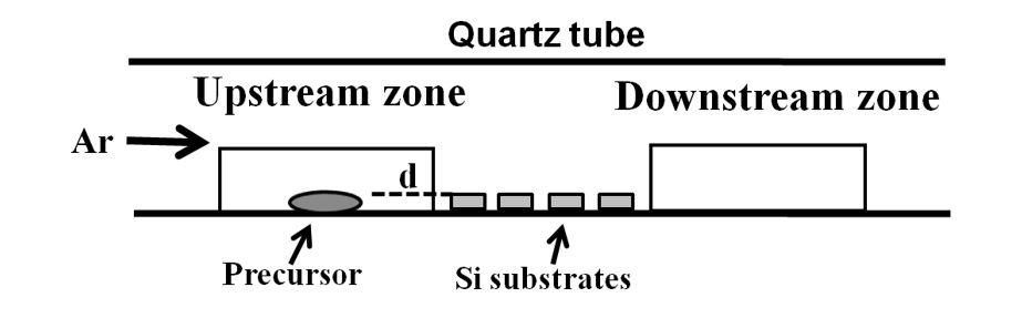
Ag2Te nanowires were grown on Si (111) substrates placed at the junction between upstream and downstream zones using a characteristic two-zone temperature furnace with an inner quartz tube (a layout in Scheme 1). The precursor, kept in an alumina boat and placed at the centre of the upstream zone, was evaporated at 1000°C with a heating rate of 50°C/minute. Figure 1(a) shows the morphology of the NWs as examined by SEM using a Philips XL30SFEG. The high magnified SEM image of a typical single NW (inset of Fig. 1(a)) and the TEM image (Fig. 1(c)) demonstrate that the NWs are clean and highly uniform. The NWs were of 10 to 15 micrometers long and 50 to 250 nm diameter. The XRD pattern of the as-grown NW ensemble (Fig. 1(b)) shows the Bragg diffraction peaks, which were indexed to the monoclinic Ag2Te structure (JCPDS file: 65-1104), denoting the growth of monoclinic Ag2Te NWs. The XRD spectrum did not exhibit any significant characteristic Bragg peak of Ag or Te metal, which excludes significant Ag/Te phase segregation and formation of Ag/Te metal clusters/precipitates in the Ag2Te nanowires. The TEM image from a representative NW with a diameter of 60 nm is shown in Fig. 1(c). The inset of the figure depicts the selected area electron diffraction (SAED) patterns of the NW. It shows a regular spot pattern, revealing the single-crystalline phase of the NW. The diffraction spots pattern were indexed to monoclinic Ag2Te structure (JCPDS file: 65-1104), in accordance with XRD pattern of NW ensemble. The NW growth direction was along (Ī13) plane. The lattice spacing (d) of 3.96 Å and 4.13 Å were identified as (011) and (Ī02) planes respectively, of monoclinic Ag2Te. Figure 1(d) depicts a HRTEM image and the clear lattice fringes confirm the single crystalline nature of the NWs. The interplanar spacing (d) perpendicular to the growth direction was estimated as 2.34 Å fitting well with the interplanar distance of the (Ī13) plane, endorsing the (Ī13) growth direction of the NWs in agreement with the SAED findings. The observed interplanar spacing is in concurrence with d = 2.31 Å of (Ī13) planes in bulk monoclinic Ag2Te.
Figure 2 depicts the EDS composition line profile measured across the diameter of the NW and the corresponding spectrum from a single Ag2Te NW. The spectrum in Fig. 2(c) illustrates that the NW consists of Ag and Te elements. The quantitative analysis indicates that the atomic ratio of Ag to Te is close to 2:1, confirming the growth of Ag2Te NWs (lines due to Cu is from the TEM grid). The composition line profile measured along the diameter of the NW (Fig. 2(b)) shows a uniform composition of Ag and Te along the cross-section of the NW.
It is noticed that Te NWs were grown on the Si substrate if the experiment was performed at an upstream temperature of 900°C or less, indicating temperature dependence on the growth of NWs. Figure 3(a) shows the morphology of nanowires as examined by SEM. The magnified image in the inset illustrates that the NWs are clean and highly uniform. The XRD pattern (Fig. 3(b) ) of the as-grown Te NW ensemble on the Si substrate shows Bragg diffraction peaks that were indexed to hexagonal Te structure (JCPDS file: 36-1452). Figure 3(c) depicts the TEM image of a typical Te NW. The upper inset in the figure depicts the SAED patterns of the NW which shows a regular spot pattern, reflecting the single-crystalline nature of the NW. The diffraction spots pattern were indexed to hexagonal Te structure (JCPDS file: 36-1452), in agreement with XRD pattern of NW ensemble. The NW growth direction was along (001) plane. The lattice spacing (d) of 2.1 Å was identified as (111) plane. Figure 3(d) depicts the high resolution (HR) TEM and the clear lattice fringes indicate that the NW is single crystalline in nature. The interplanar spacing (d) perpendicular to the growth direction was estimated as 5.92 Å fitting well with the interplanar distance of the (001) plane, confirming the (001) growth direction of the NWs. The relevant Fast Fourier transformation pattern is shown in the inset of Fig. 3(d). The EDS spectrum obtained from the marked portion on panel ‘c’ is shown in the lower inset of Fig. 3(c), which confirm that the NW consists of only Te element (lines due to Cu is from the TEM grid).
To deduce a possible NW growth mechanism systematic experiments were carried out at various upstream temperatures and flow rates. Subsequently, EDS analysis was performed at each stage to determine the type of NWs (i.e. whether the grown NWs are Te, Ag or Ag2Te). It is found that Te, Ag2Te or a mixture of Te and Ag2Te NWs were grown on the substrate, depending on the upstream temperature whereas the flow rate has negligible effect. Further, EDS analysis was also carried out at several spots on the same substrate deposited at each upstream temperature to determine the type of NWs formed. It is observed that the percentage of Ag2Te NWs increases with temperature whereas that of Te NWs shows the opposite trend. For example, Te NWs were grown for an upstream temperature equal to 900°C or less. In contrast only Ag2Te NWs dominate in the temperature range 1000–1050°C. In the intermediate temperature at 950°C, EDS analysis indicated the presence of both Te and Ag2Te compound on the substrate.
This strong dependence of the Te and Ag2Te NWs percentage on the temperature can be explained in the following way. Ag2Te compound is known to start to dissociate even at temperatures as low as 750°C, depositing mostly Te on the substrate at low temperature [24]. This is because the evaporation rate of Te atoms is greater than those of Ag atoms and Ag2Te molecules. The strong reactivity of Ag and Te ((G Ag2Te)298 = -81.66 kJ mol− 1) is also known [25]. Thus during the heating of Ag2Te powder in the upstream, the precursor dissociates and the vapors of Ag and Te carried over to the downstream of the apparatus by the Ar carrier gas recombine on the Si substrate to form Ag2Te nuclei, which may act as seeds facilitating the growth of Ag2Te NWs. The nucleation of Ag2Te from Ag and Te elements requires diffusion of the two species. It is also well known that the diffusivity of Ag in Te (4×10⁵ Å2/s at 300 K) is larger than that of Te in Ag (2.429×10− 12 Å2/s at 300 K) [26]. Therefore the structure and phase formation of the material grown on the substrate must be dictated mostly by the diffusion of Ag in Te lattice. The sequential growth of Ag2Te nanocrystals by diffusion and the phase formation was earlier studied by high resolution transmission electron microscopy [27].
When the experiment is performed at low temperatures, transportation of Te after dissociation of the precursor is favored and hence the growth of Te NWs dominates at temperatures ≤ 900°C. As the temperature increase, the evaporation rates of both Te and Ag increases so that a mixture Te and Ag2Te was obtained on the Si substrate. The vapor pressure data for pure Ag and Te suggests that vapor pressure of silver increases faster with temperature than that of tellurium [24]. Hence it seems that at our experimental condition of 1000–1050°C, after the deposition of Ag and Te atoms on the substrate, Ag2Te NWs have grown by self-seeded process through diffusion and reaction.