Double-transfer technique for top-emitting thin-film VCSELs mounted onto an aluminum substrate
The p-on-n structures of top-emitting 940-nm thin-film VCSELs are epitaxially grown on n-GaAs substrates in upright order using MOCVD, as shown in Fig. 2. Compared to the conventional p-on-n structures of bulk VCSELs, the p-on-n structures of thin-film VCSELs included additional layers, such as the etch stop layer and n-GaAs contact layer, while the p-GaAs contact layer, MQWs, two oppositely doped n-, and p-DBRs remained unchanged (see methods). The etch stop layer was inserted to keep the epilayers of thin-film VCSELs intact during the removal of a GaAs substrate in NH4OH-based etchant. The heavily n-doped GaAs ohmic layer can enhance the electrical characteristics of thin-film VCSELs as a way of alleviating the electrical loss stemming from the considerably thick and moderately doped GaAs substrates17.
Figure 3 shows the fabrication procedures of thin-film VCSELs onto an aluminum heatsink via a double-transfer technique. The double-transfer technique that transferred the thin-film VCSELs onto foreign substrates twice was carried out as follows: Figure 3(a) shows that the p-on-n structures of top-emitting 940-nm thin-film VCSELs, including the etch stop layer and n-GaAs ohmic layer, are grown via MOCVD in upright order. Figure 3(b) shows the finished front processes of thin-film VCSELs, including mesa etching, p-metal deposition, and selective oxidation of AlxGa1-xAs before separating thin-film VCSELs from the growth substrate. A Mesa etching of n- and p-DBRs and MQWs was carried out in order to isolate the VCSELs. A grid pattern of p-ohmic contact with a combination of Ti/Pt/Au was deposited on the highly p-doped GaAs layer. The 10-μm oxide-confined aperture of each VCSEL was defined with selective oxidation of AlxGa1-xAs with high Al contents. Figure 3(c) shows the thin-film VCSELs mounted on a polyimide carrier by using adhesive wax. Adhesive wax was uniformly applied on the polyimide carrier at low temperature, which was bonded to the thin-film VCSELs with controlled pressure. The highly n-doped GaAs ohmic layer is exposed after removing the GaAs substrate and etch stop layer, as shown in Fig. 3(d). The etch stop layer was selectively etched after the GaAs substrate removal, which prevented the NH4OH-based etchant from penetrating into the n-GaAs ohmic layer of the thin-film VCSELs during removal of the GaAs substrate. Figure 3(e) shows the wax-bonded thin-film VCSELs mounted onto an aluminum heatsink. After a combination of AuGe/Ni/Au was deposited on the n-GaAs ohmic layer, the wax-bonded thin-film VCSELs were integrated with silver-filled epoxy onto the aluminum heatsink. The wax-bonded thin-film VCSELs were completely bonded onto the aluminum heatsink during the curing of the silver-filled epoxy at 150 ℃ for one and a half hours. Figure 3(f) shows the top-emitting 940-nm thin-film VCSELs transferred onto the aluminum heatsink using the double-transfer technique. The polyimide carrier was separated by selectively removing the wax, thereby the top-emitting 940-nm thin-film VCSELs mounted onto the aluminum substrate were successfully fabricated.
Operation of top-emitting 940-nm thin-film VCSELs with p-on-n polarity
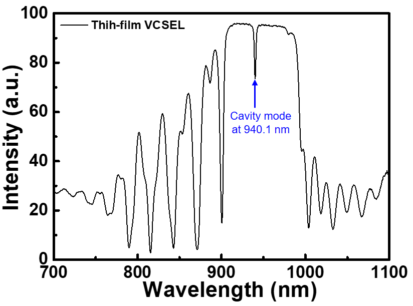
Figure 4(a) shows a top-view scanning electron microscopy (SEM) image of the fabricated 940-nm top-emitting thin-film VCSELs onto the aluminum heatsink. The surface of the thin-film VCSELs mounted onto the aluminum heatsink was considerably smooth. Figure 4(b) shows the cross-sectional SEM image, obtained using focused ion beam (FIB) milling, of the fabricated thin-film VCSELs where the n- and p-DBR layers as well as the MQWs are clearly visible. No significant dislocations of the transferred thin-film VCSELs onto the aluminum heatsink were observed in the VCSEL structure, demonstrating the feasible double-transfer technique for transferring the thin-film VCSELs onto foreign substrates. Figure 4(c) shows an optical microscopy image of the fabricated 940-nm top-emitting thin-film VCSELs onto the aluminum heatsink using a probe station. The invisible laser emission of the 940-nm thin-film VCSELs at injection current of 8 mA was observed to be a purple beam using a conventional microscope5. As can be seen from Fig. 4(d), the peak wavelength of the emitting light from the thin-film VCSELs was 941 nm which corresponded to the sharp reflectance dip near 940 nm shown in Supplementary Figure S1.
Figure 5 shows the L-I-V characteristics of the thin-film VCSELs onto the aluminum heatsink. The dot-dashed line indicates the threshold current of 1 mA. The peak power of the thin-film VCSELs was 7.7 mW at input current of 16.1 mA. A few deformations of contact layers, as shown in the SEM image of Fig. 5, might contribute to an increase in series resistance, resulting in a rather high threshold voltage of approximately 2.8 V and steeper upward tilt to the slope of the I-V curve of thin-film VCSELs.